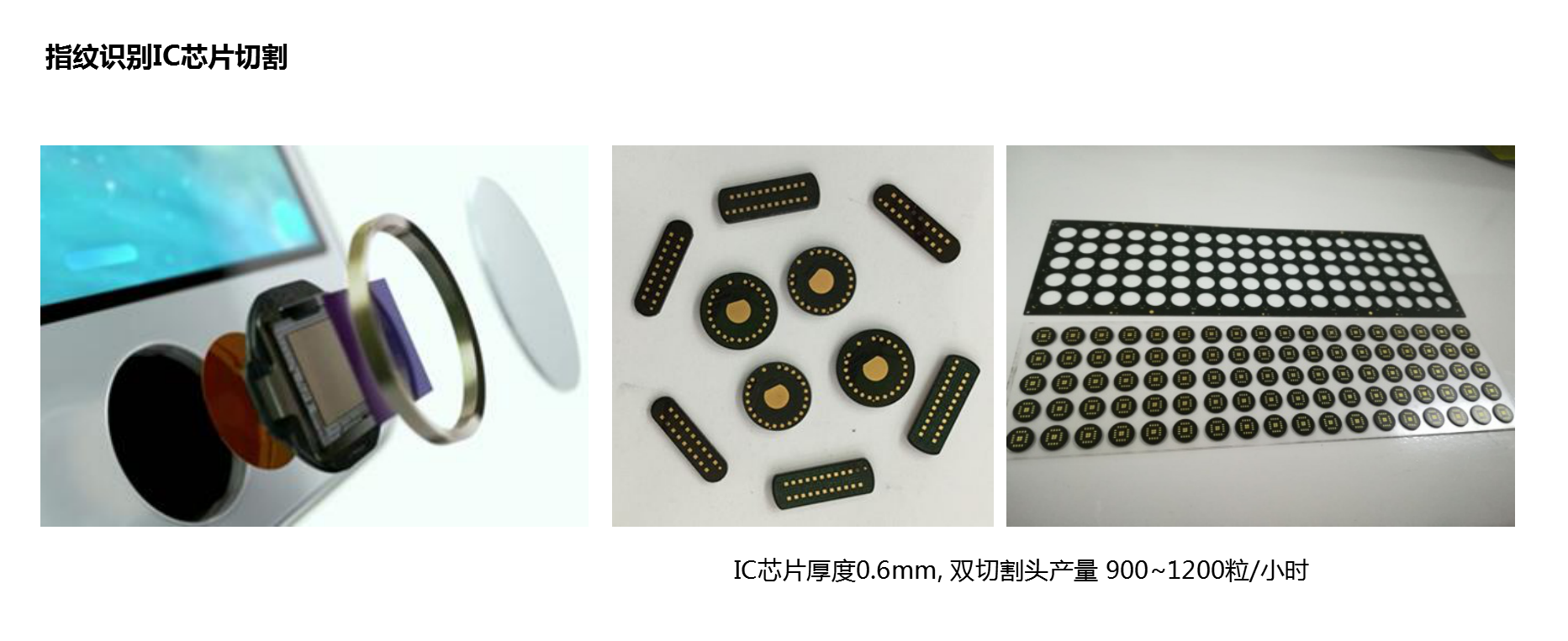
The semiconductor material process is developing from the first-generation single-element semiconductor to the second- and third-generation semiconductors such as gallium arsenide (GaAs), gallium nitride (GaN), and silicon carbide (SiC). The update of emerging materials brings about new requirements and challenges.
The chip needs to be obtained by dividing a sub-unit (a chip particle) on the wafer. "Wafer dicing process" refers to dicing or grooving the wafer or its components to facilitate subsequent process or functional testing. "Wafer dicing" requires high cutting accuracy. Wafers are made of ultra-brittle materials, and the control of positive and back collapse is also very strict. Wafer products are high value-added products, and the reliability requirements of dicing equipment are also very high.
As the semiconductor manufacturing process becomes more and more sophisticated, the manufacturing cost is getting higher and higher, so the industry puts forward higher requirements for the product utilization rate of single wafers.Laser scribing can make chip layout finer, and the processing process is cleaner and more efficient. Laser scribing has become an important means for semiconductor companies to improve product production efficiency and production quality.
Especially for some wafers or chips containing low-k materials, their soft structure and easy permeability make CMP (Chemical Mechanical Polishing) and cleaning procedures more difficult, resulting in a decline in yield and an increase in production costs.Strong Laser's ultra-fast laser system for wafer has the advantages of accurate cutting, small heat-affected zone, non-contact processing, no cleaning process, no secondary pollution, etc. It is the first choice in the industry.
Strong laser picosecond laser scribing system compresses the Gaussian laser beam to the diffraction limit through a Bessel or DOE optical system. Under the action of a laser beam with a high repetition frequency of 100-200kHz and an extremely short pulse width of 10ps, the focused spot diameter is as small as 3μm, with a very high peak power density. When it is focused inside the transparent material, it instantly vaporizes the material in this area to produce a vaporization zone, and diffuses up and down the two surfaces to form a nonlinear crack, thereby cutting and separating the material. Common transparent materials including glass, sapphire and semiconductor silicon wafers (infrared radiation can transmit semiconductor silicon materials) are suitable for picosecond & femtosecond laser scribing.

Strong laser dicing solutions for wafer has significant advantages in wafer dicing and dicing processing of various shapes. For example, there is no need for an additional wet cleaning process during the processing, which completely avoids secondary pollution and physical damage to the inner and outer surfaces of the semiconductor device. The degree of production automation is high, and the production efficiency and production yield are fully guaranteed. Compared with the traditional cutting process, it has the following advantages: narrow cutting gap, small deformation of the workpiece, non-contact processing, adaptability and flexibility.
Main equipment:Strong laser picosecond scribing machine for wafer