HDI high-speed circuit boards need to meet the requirements of large broadband and large-capacity data transmission. This requirement has become mainstream in the field of mobile smart terminals. The characteristic of HDI circuit board is that there are many micro blind hold/buried blind hold, which are generally realized by adding layers. According to the number of layers, HDI can be divided into first-order HDI, second-order HDI, third-order HDI, and arbitrary layer HDI (Anylayer HDI is the highest-order HDI).
The main feature of HDI high-speed circuit boards is high density. HDI has many micro-blind holes/buried blind holes, so its wiring density is higher than that of through-hole plates. The principle is that blind holes/buried blind holes can save wiring space. Common multi-layer boards use through holes to connect different layers, but the through holes will occupy a lot of space that can be used for wiring. On the contrary, blind holes/buried blind holes are used to achieve the connection function between different layers, which can make room for more Wiring, thereby increasing the density of wiring.
Therefore, the more blind holes/buried blind holes of HDI, the higher the density, and the higher the order of HDI.Anylayer is the highest density board type in HDI . It is worth noting that Anylayer can’t increase the wiring density by adding blind hole /buried blind hole. Therefore, base on the HDI process in industrial manufacturing, people introduce the semi-additive method (mSAP) and carrier board to manufacture higher-density boards, that is, Substrate-like PCB (SLP). It can be seen that HDI is an important board for high-density wiring.
Strong uses galvanometers and field lenses to focus high-peak power lasers on the surface of the material and repeat the circular motion many times. The surface of the material is gradually etched from top to bottom. The material is heated instantly to the vaporization temperature and escapes from the surface of the material in the form of gas.


Major equipment:Strong laser cutting machine by femtosecond & picosecond ultrafast、Strong laser UV picosecond cutting machine for cover film
Strong Laser is dedicated to find solutions for laser drilling of circuit boards. It uses the extremely high peak power of the picosecond laser to conduct a huge amount of energy to the surface of the material in a short time by means of a single pulse accumulation or multiple pulse spiral motions, so that the material is melt and evaporate instantly. In this process, the volume of the material in the hole expands sharply, generating tremendous pressure . This pressure pushes the denatured material out of the hole. Because the thermal effect of picosecond laser is very small , comparing with the CO2 laser, the roundness of the hole is smoother and the edges are more neat.
Major equipment:Strong laser HDI drilling machine in high-speed
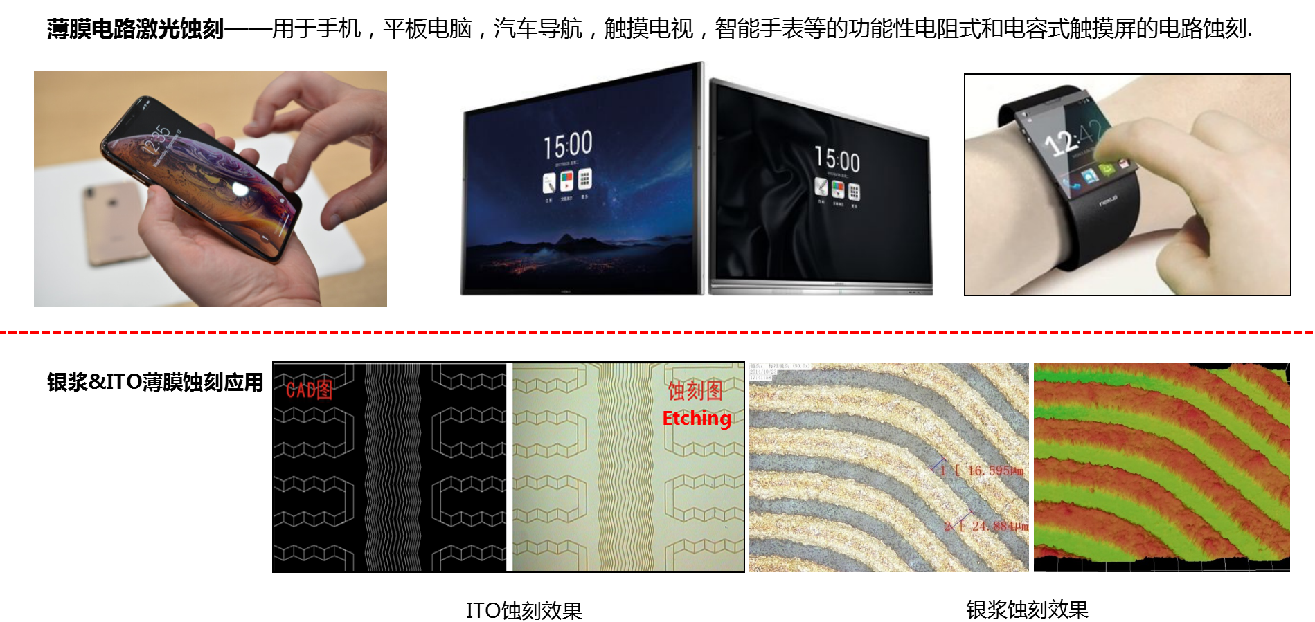
For the etching solution of the circuit board, Strong Laser uses a laser beam with high beam quality but low power to focus into a very small spot. So that the metal circuit generates a high temperature at the focal point and then vaporizes instantly. This solution is mainly used for HDI circuit copper clad copper layer circuit production, thick copper plate PAD laser drilling copper layer opening, PCB printed conductive ink circuit production, FPC calendered copper copper layer circuit production, FPC printed conductive ink circuit production, etc.

The laser etching solution has the following excellent processing characteristics: non-contact processing, high degree of flexibility, high efficiency, no noise, small heat-affected zone, and can be focused into a very small spot (laser wavelength level), etc. These can obtain good dimensional accuracy and processing quality of drilling, dicing, etching and cutting. In particular, the interaction with certain materials (such as polyimide) is a "cold working" of "photochemical action", which can obtain the effect of non-carbonization. This is widely used in the processing of electronic semiconductor materials.
Major equipment:Strong laser etching machine for thin film circuit with Single/double head 、Strong laser etching machine with ultra large format