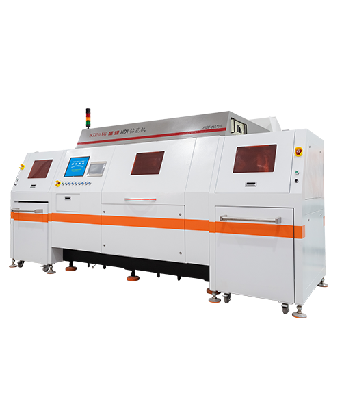
Model:SLZK-8070I-PCB
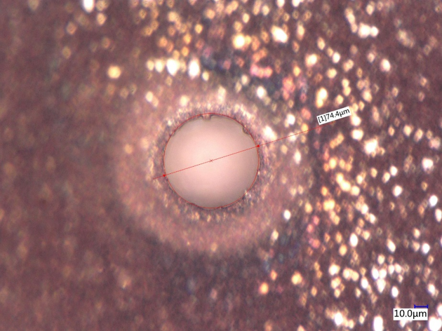
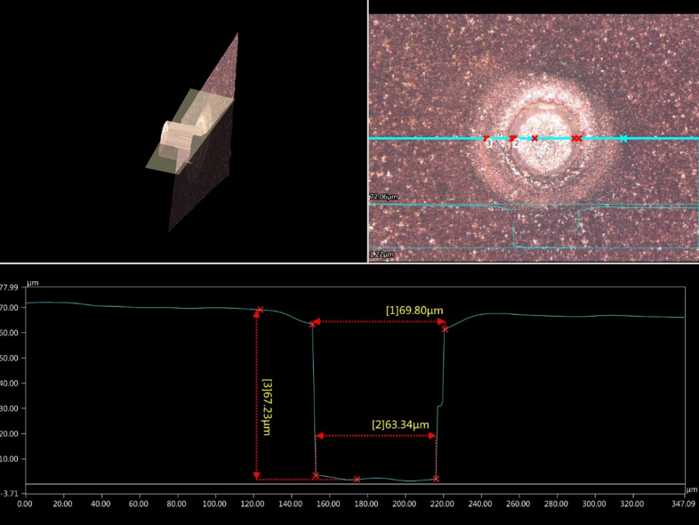
Application:PCB multilayer interconnection board drilling blind holes, chip-to-chip mode
Nanosecond laser-hot melt processing, this process relies on the thermal accumulation of laser energy to melt and even volatilize the material. The pulse duration is long, which leads to heat accumulation and conduction in the material and has a large thermal influence to the edge of the processed material. It is easy to produce slag and debris.
Picosecond & Femtosecond Laser——The principle of this process is vaporization and ablation or modification processing. Its pulse width is extremely short. It relies on its own extremely high peak power to instantly gasify the material, with minimal thermal effect and no melting beads. The processing edges are neat.
| No. | Item | Index |
|---|---|---|
| 01 | Laser type | 515/532nm ps |
| 02 | Laser power | 90W |
| 03 | Drilling accuracy | ±20um |
| 04 | Efficiency | 1200 holds/head/s (90um) |
| 05 | Software | Strong self-developed control software |
| 06 | CCD visual positioning system | CCD vision automatic positioning, size compensation, field of view range 6*8mm |
| 07 | X, Y linear motor motion platform | 850X700mm 800mm/sacceleration |
| 08 | X, Y platform positioning accuracy | ±1.5um |
| 09 | Scanning range of galvanometer | 50x50mm |
| 10 | Process method | Large Window / Conformal Mask / Cu Direct |
| 11 | Automatic loading and unloading time | Within 12 seconds |
| 12 | Size | 4080X2270X2000(mm) |
| 13 | Consumption | 20KW |


 0769-83131319
Tel:0769-83131319
Add: No.21,Dalang Xinbao 2nd Street,Dalang Town,Dongguan City,Guangdong Province
Tel:15312164555
Add: Building 8, No. 200 Shengpuxing Road, Suzhou Industrial Park
 0769-85641965
Tel:0769-85641965
Add: 2nd Floor, Building 3, Kusai Technology Park, No. 8 Fumin South Road, Dalang Town, Dongguan City
Tel:15312164555
Add: Building 8, No. 200 Shengpuxing Road, Suzhou Industrial Park


